When : Thursday, 12 March from 2.30 to 3.30pm (CET) – Open seating as from 2.15pm
Speakers : CERN’s Director General, Rolf Heuer and Director of Accelerators, Frédérick Bordry, and representatives of the LHC experiments
CERN is pleased to invite you to the above press briefing which will take place on Thursday 12 March, in the Globe of Science and Innovation, 1st floor, from 2.30 to 3.30pm (CET).
The Large Hadron Collider (LHC) is ready to start up for its second three-year run. The 27km LHC is the largest and most powerful particle accelerator in the world operating at a temperature of -217 degrees Centigrade and powered to a current of 11,000 amps. Run 2 of the LHC follows a two-year technical stop that prepared the machine for running at almost double the energy of the first run. After substantial consolidation and improvements the LHC will restart at an energy of 6.5 TeV per beam, which will open up a new window for discovery – collisions at a total energy of 13 TeV are expected late Spring.
CERN General Director Rolf Heuer, the Director of Accelerators Frédérick Bordry, and the LHC experiment representatives will take questions regarding the LHC second three-year run, focussing on the technical challenges in preparing for Run 2, and on the new discovery potential.
LHC experimental physicists and theorists will be at your disposal for interviews at the end of the briefing. The highlight of the machine’s successful first run was the discovery by the ATLAS and CMS experiments of the long-sought Higgs boson.
CERN, the European Organization for Nuclear Research, is the world’s leading laboratory for particle physics. It has its headquarters in Geneva. At present, its Member States are Austria, Belgium, Bulgaria, the Czech Republic, Denmark, Finland, France, Germany, Greece, Hungary, Israel, Italy, the Netherlands, Norway, Poland, Portugal, Slovakia, Spain, Sweden, Switzerland and the United Kingdom. Romania is a Candidate for Accession. Serbia is an Associate Member in the pre-stage to Membership. India, Japan, the Russian Federation, the United States of America, Turkey, the European Union, JINR and UNESCO have Observer Status.
MAGIC project leader at the Max-Planck-Institute for Physics, Munich, and spokesperson of the MAGIC Collaboration.
You are Project Leader and Spokesperson for the MAGIC collaboration. What are the major goals and research directions of the collaboration?
The Imaging Atmospheric Cherenkov Technique (IACT) has made giant steps – in fact it became a powerful new branch of astrophysics. With the discovery of very high energy (VHE) gamma rays from the Crab Nebula in 1989, the Whipple team laid the foundation for the new science. Other telescope installations, like HEGRA and CANGAROO, belonging to the so-called 2nd generation IACTs, very soon started their own search of gamma ray sources. Although some 10 sources were discovered by the year 2000, still all of those detections were made above the energy threshold of ~300 GeV.
Already in 1995, at a few conferences, we had presented the concrete concept of the 17m diameter MAGIC telescope. Shortly before we had understood that the energy threshold of detection (Ethreshold) was inversely proportional to the area of the mirror (1/√Amirror) and not the square root of the area as is the case for non-imaging telescopes, showing thus that one can build a moderately large diameter telescope for operating in the domain of sub-100 GeV energies.
The MAGIC design was aiming to go towards the sub- 100 GeV energy range down to 30-40 GeV, into the last decade, “terra incognita” of the electromagnetic emission spectrum, traditionally considered as the classical domain of satellite-born instruments. MAGIC people were anticipating finding new classes of sources such as, for example, the pulsars. Also, because of strong absorption of TeV gamma-rays by the extragalactic background light, MAGIC was aiming to measure sources in the sub-100 GeV range, where the universe is much more transparent to gamma rays and one can search for powerful sources located at large redshifts.
We have spent a lot of effort planning the telescope to be light-weight, for fast repositioning of the telescope in response to the alerts os satellites spotting Gamma Ray Bursts, trying to measure them still in the prompt phase of the emission. For that purpose we built the reflector of the telescope from reinforced carbon fibre, which is several times lighter than the steel but has a comparable stiffness and very low thermal expansion. For the same reason we introduced the concept of the Active Mirror Control to the VHE Gamma Astrophysics, allowing one to counteract the deformations of the reflector due to varying gravitational loads when tracking sources.
Today we are happy that our expectations were largely fulfilled. In 2008 we found the first pulsed signal from the Crab pulsar at energies above 25 GeV, for the first time creating a bridge between satellite detectors and IACTs. Recently we found that the spectrum of the pulsating gammas from Crab is extending till ~2 TeV, i.e. that an object of a ~ 10km size can accelerate electrons to a gamma factor of ~ 107. By using the data of the Fermi satellite and of MAGIC we measured very precisely the peak position of ~ 55 GeV of the Inverse Compton emission of the Crab Nebula. Recently, via gravitational lensing, we found the new source S3 0218 located at a redshift of almost 1 (z=0.944). The list of highly interesting results, both of extragalactic and galactic origin, is really long and it is progressively updated with newer results.
Both ETE and Hamamatsu went through several development iterations, consequently improving the key PMT parameters, one at a time. Left: two 8-dynode PMTs from ETE of intermediate types D872 and D569/2SA, clear input window. Right: PMT R12992-100 (7-dynodes) and R11920-100 (8-dynode) from Hamamatsu, both of mat window type. The final 7-dynode PMTs from both companies will be compatible in pin, size and window type.
Could you give a brief overview on light sensor technology used in astroparticle physics?
The classical photomultiplier tubes (PMTs) are the main detectors used as light sensors in astroparticle physics experiments. In a dedicated two-stage development program (at first for MAGIC and since 2010 for the CTA collaboration), in tandem with industrial partners Hamamatsu (Japan) and Electron Tubes Enterprises (England), we succeeded to significantly improve the performance of PMTs. Today we arrived at 1.5 inch size commercial PMTs for the CTA project, which have an average peak quantum efficiency (QE) of ~40%, photo electron collection efficiency in excess of 95%, and about 50 times reduced after-pulsing. Now these are the best PMTs worldwide. We anticipate that these novel technologies will be applied also to the large size PMTs, much needed in neutrino experiments.
Silicon photomultipliers (SiPMs) emerged as novel photo sensors some 15 years ago. In 2003 we suggested to use them in astroparticle physics experiments, initially in EUSO and in MAGIC, and actively participated in their development. Some seven years ago we started constructing realistic pixels for IACTs. This initiative has been taken by our colleagues from the FACT collaboration that succeeded constructing a full-scale operational camera. My colleagues from the CTA collaboration are planning to use SiPMs for the cameras of the so-called small size telescopes (~4m diameter class) as well as for the mid-size Schwarzschild-Couder telescope. The parameters of SiPMs are still improving, every 6-8 months we face novel and better products from several manufacturers. For the time being the best SiPM samples come close to the parameters of the best PMTs. The SiPMs have the potential to achieve a photon detection efficiency (PDE) of ~60-65% at an acceptable low cross-talk level of a few percent; this may be within reach within the next couple of years. The SiPMs have a small size of typically 3mm×3mm or 6mm×6mm. The limitation on the size is due to the requested fast timing of a few nanoseconds, as well as, due to the increasing with size gain and cross-talk. Currently a few groups are trying to build close-packed matrixes of SiPMs for emulating PMTs of 1-1.5 inch size, but the results still need to be carefully evaluated.
Since a few years several manufacturers offer integrated matrixes of SiPMs. The final goal will be to arrive at optimized in performance, ns-fast matrixes, which will include on the rear side the readout of the measured charge, similar like today’s CCD and CMOS cameras do. Given these, one can assemble, as Lego, high-resolution imaging devices of arbitrary size and shape. These will revolutionize not only the physics experiments but also the imaging devices in medicine and will find extremely wide applications everywhere.
What are the main innovations/technological improvements in the use of light sensors in astroparticle physics?
Since the mid 1960’s the main parameters of PMTs were stagnating for about 40 years. The main innovation in light sensors in the past 10 years are related to the enhancement of their photon detection efficiency and the suppression of the unwanted after-pulsing in PMTs and cross-talk and after-pulsing in SiPMs. About 10 years ago the typical PMT had a peak QE of ~25%, photo-electron collection efficiency of 80% and an after-pulsing level of 0.5% for the set threshold of 4 photo electrons. Today we have PMTs with peak QE in excess of 40%, photo electron collection efficiency of 95-98% and an after-pulsing below 0.01%.
A faster improvement can be observed for SiPMs. While SiPMs from Hamamatsu, named MPPC (multi-pixel photon counter), were showing a peak PDE of 30-35% ~5 years ago, today there are devices with a peak PDE of ~45%. But for the majority of experiments the PDE of SiPMs alone is not a very meaningful parameter; one needs to consider the cross-talk and the after-pulsing levels for understanding the limitations in the aimed application. Today SiPM samples from several manufacturers show cross-talk at a several percent level; this is to be compared with their one order of magnitude higher level in the relatively recent past.
Today SiPM cost is becoming progressively low. This is unfortunately not the case for the readout systems. For planning an astroparticle physics detector one needs to carefully consider costs. Even with comparable photon detection efficiencies of SiPMs and PMTs, simply substituting the PMTs by assembled matrixes of many SiPMs may not necessarily offer an optimal solution. In addition, the assembled matrixes of SiPMs may not be as fast as the PMTs; also, it is well known that even a single SiPM has a significantly higher noise rate than a PMT. But as I mentioned earlier, the SiPM parameters are still improving and when their PDE will exceed that of PMTs by ~50%, they may become very strong competitors for PMTs, albeit only for small sensor size applications.
What are the technological advances in ground-based gamma-ray astronomy? And what are the upcoming plans?
The technological advances in ground-based gamma-ray astronomy are multi-fold, they can be observed taking as an example the (differing in size and performance) telescopes of the CTA collaboration:
Use of novel technologies for mirror production providing longevity (mirrors currently used for IACTs are strongly deteriorating after ~3 years).
The Active Mirror Control System finds wide application in large-size telescopes. This provides optimal focusing of telescopes independent on observation angles.
Novel readout systems in the imaging cameras provide an order of magnitude lower cost compared to what was used just a few years ago.
We are moving towards sealed, temperature-controlled imaging cameras; this is necessary for the desired robotic operation of the telescopes in the future and for the reduced maintenance of multiple telescopes in high-mountain altitude or desert locations.
Double-mirror telescope designs are paving the road. They are using SiPM-based cameras, offer a compact design for a wide field of view and promiss an improved angular resolution. The main challenges here are related to the secondary mirror which needs high precision both in quality and fixation in the structure. The first ASTRI telescope of the Italian INAF was inaugurated in Sicily in September 2014. Probably within a time scale of a year we will have results from the first measurements. The main problem with the double-mirror designs, compared to simple prime focus telescopes, is their high cost.
Speaking about future plans, I believe that the last word in the scene of light sensors is not yet said, not only the SiPM but also the PMT parameters can still be improved significantly. I am part of a small community of photo-cathode-related specialists-enthusiasts who are dreaming about a PMT with peak QE as high as maybe 70% (for the time being we have few samples of 45-47%). For me, this is essentially linked to the question of availability of financial resources and coordinated efforts of a few years.
You are heading a Russian-German collaboration at Tunka Valley, operating a large-scale experiment studying cosmic rays and gamma-rays. Could you say something about this project and its expected outcomes?
The experiment dubbed as TAIGA in Tunka valley, near the lake Baikal, is really interesting. Currently TAIGA has an operational 185 station TUNKA open-air-integrating Cherenkov detectors. An underground muon detector is under construction for vetoing muons. The experiment is hosting an array of radio detectors from our colleagues from Karlsruhe.
Our idea is to try to operate a single small-size, wide-angle imaging Cherenkov telescope together with the wide-angle integrating Cherenkov detectors (dubbed HiSCORE), which (initially) will be spread over a distance of ~600 m from the telescope. This combination can be considered as a “cell” of a future large-size instrument. Since some time now, the concept of HiSCORE, along with that of the imaging telescope, is pursued by my colleagues from the University of Hamburg and DESY (from Hamburg and Zeuthen locations), together with experienced research teams from MEPhi, SINP MSU, ISU and JINR Dubna in Russia. The combination of a low-coat wide-angle imaging Cherenkov telescope with the so-called HiSCORE detectors, spread over large distances, has the promise to offer very large collection area for measuring the spectra of tens of TeV to hundreds of TeV gamma-ray sources (so called PeVatrons). Compared to planned alternatives, this is a really low-cost detector. We will try to prove this principle in the coming years. Some 30 HiSCORE stations are now operational and the first imaging telescope is under construction.
Further reading:
HEGRA: The High Energy Gamma Ray Astronomy experiment was located on La Palma (Canary Islands) at a height of 2200 m. It consisted of several detector types for observing secondary particles or light from cosmic ray particle cascades in the atmosphere, in the energy range 1012 to 1016 eV. The strongest detector of HEGRA was the array of six ~4m class IACTs. HEGRA was taking data between 1987 and 2002. CANGAROO III: Collaboration of Australia and Nippon (Japan) for a Gamma-Ray Observatory in the Outback. The experiment uses an array of 4 imaging atmospheric Cherenkov telescopes in Australia. CTA: Cherenkov Telescope Array is an initiative to build the next generation ground-based very high energy gamma-ray instrument. CTA is included in the 2008 roadmap of the European Strategy Forum on Research Infrastructures (ESFRI), is one of the “Magnificent Seven” of the European strategy for astroparticle physics published by ASPERA, and highly ranked in the “strategic plan for European astronomy” of ASTRONET.
A.M. Hillas, “Evolution of ground-based gamma-ray astronomy from the early days to the Cherenkov Telescope Arrays”, Astropart. Phys., 43, (2013), 19-43
E. Lorenz, R. Wagner, “Very High Energy Gamma-Ray Astronomy. A 23 Year Success Story in High Energy Astroparticle Physics”, Europ. Phys. J. H, 37, 3 (2012) 459-513
R. Mirzoyan, “Brief History of Ground-Based very High Energy Gamma-Ray Astrophysics with Atmospheric Air Cherenkov Telescopes”, Astropart. Phys., 53 (2014) 91-99
Dr. Razmik Mirzoayn is permanent staff member at the Max Planck Institute for Physics in Munich, the current Spokesperson of the MAGIC collaboration and the Principal Investigator and Spokesperson of the TAIGA collaboration. He is honorary professor and head of the laboratory “Multi-TeV Energy Gamma-Ray Astronomy” at the Irkutsk State University in Russia. He recently became foreign member of the National Academy of Sciences of the Republic of Armenia.
Dr Mirzoyan is one of the founders of the HEGRA IACT system, one of the founders of the MAGIC telescopes system, and has strongly contributed to CTA, especially in the design of the imaging cameras. He has strong interest in light sensors, in developing PMTs, HPDs and SiPMs.
He received his PhD (1985) from the Lebedev Physics Institute of the Academy of Sciences of USSR in Moscow. He is author/co-author of over 500 publications (over 200 in peer-reviewed journals) and he is co-authoring six patents.
Submitted by Eleni Chatzichristou
APPEC Communications Officer
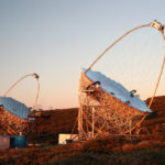
The two MAGIC telescopes at the Roque de los Muchachos Observatory on the Canary island of La Palma (Max Planck Institute for Physics/R. Wagner).
by Razmik Mirzoyan MAGIC project leader at the Max Planck Institute for Physics, Munich, and spokesperson of the MAGIC Collaboration
Both MAGIC telescopes were upgraded about 2.5 years ago and now they are running with 1039 fine pixel (0.10°) cameras in the coincidence (stereo) mode. The standard trigger provides an energy threshold of ~ 50 GeV. Currently we are evaluating the results of the SUM-Trigger, which allows us lowering the trigger threshold down to ~ 35 GeV. Now both telescopes are using a 1.64 GSample/s readouts based on DRS4 chips. During last summer we changed about one third of the mirrors on the MAGIC-I telescope, which were in operation since 2004, and also a small number of mirrors on the MAGIC-II telescope. I have been involved with the MAGIC telescopes since the very first days of their operation and I can say with certainty that these were never in such a good shape as they are now.
All researchers involved in the collaboration are really enjoying pointing the telescopes to the skies and picking sources to find, sometimes unexpectedly, highly interesting results. Last year we were literally flooded by novel results and, although we published a really large number of peer-reviewed papers, we still have almost triple as many results in the publication queue. Trying to cope with this situation, we have introduced the position of “publication manager” whose sole task is to accelerate the publications. What I find very interesting and pleasing is the large flux of young female researchers who are in increasingly large numbers joining our collaboration, obviously attracted by the very dynamic research.
Just to name a few highly interesting results, recently we succeeded in measuring the pulsations from the Crab pulsar, extending to at least 2 TeV, and we could not observe any tailing off of the spectrum yet. Even a few years ago nobody could imagine this. In a series of five papers (the fifth one is under review for publication) on the same Crab pulsar, spread over the last several years, we could experimentally measure several very novel features: e.g. the spectrum starting from 25 GeV and extending to TeV energies, indicating extreme acceleration of electrons in this compact object (the size of a pulsar is estimated to be ~ 10km), the existence of the bridge component of the emission at higher energies, very sharp pulse time profiles, inverse-Compton scattering mechanism for energies above 10 GeV, and many other interesting features.
From qualitative measurements we moved to precision measurements of the parameters of the Crab pulsar, providing accurate input for novel theories. I should mention that with every next measurement of MAGIC we showed that none of the existing or currently developed novel theoretical models was able to satisfactorily describe the experimental data. In my opinion the pulsars, along with the black holes, are the most complex objects in the sky. We are anticipating novel, quantitative theory models to appear in the next years, which can be tested with our experimental measurements.
Another example of highly interesting results, is our recent finding of the most distant source at VHE energies, S3 0218 at a redshift of 0.944. We detected the delayed flare from this object, due to gravitational lensing, 11 days after the first alert reported by the Fermi satellite mission. So with this measurement we doubled the redshift reach of IACTs. The physics implications of this detection are still under evaluation.
I want also to mention our recent article on a big flare from the radio galaxy IC 310, which appeared in the SCIENCE magazine. The ~ 5 minutes signal variability received from this object was about five times shorter than the size of the event horizon of the black hole residing in IC 310. We suggested a novel theoretical model, a pulsar like mechanism for the black hole, in order to explain this unusual behavior.
We are confident that the next five years will be the most productive time in the history of MAGIC and that we will continue to strongly contribute to the physics of cosmic rays, astroparticle physics and cosmology. We are looking forward to the exciting future of ground-based gamma-ray astronomy, which soon will be crowned by the CTA arrays.
Senior Marie Curie Research Fellow at the Dept. of Physics, University of Liverpool and the Cockcroft Institute of Accelerator Science and Technology, UK
Could you give a brief overview of SiPM applications?
The first project on Silicon Photomultiplier (SiPM) applications were conducted by MEPhI-Pulsar-ITEP-DESY team in 2003-2005 where a few thousand SiPMs were used as readout of the wavelength-shifting fibre tile calorimeter for the CALICE collaboration. It confirmed the possibility of using SiPM in large scale scientific experiments. A first large industrial-scale project of SiPM implementation was an upgrade of the T2K neutrino detection system in Tokai-to-Kamiokande, Japan. About 60,000 SiPMs were supplied by Hamamatsu and have been successfully tested and assembled by the T2K collaboration since 2006. T2K experiment has been started in 2009, and observation of neutrino oscillations has been reported in 2011. There are a number of accelerator upgrade projects under consideration now, including beam loss monitoring systems for the Large Hadron Collider at CERN, future linear colliders and light sources, detector systems of the CMS HCAL, ALICE and NA61/SHINE high energy physics experiments, calorimeter systems at Fermi Lab and Jefferson Lab (USA).
Medical imaging is another very attractive industrial-scale area of SiPM applications. Now, major vendors of Positron Emission Tomography (PET) scanners, including General Electric, Siemens and Philips, as well as a number of academic-industrial collaborations, e.g. within the EU funded projects “Hyper Image”, Endo TOFPET, the AX-PET collaboration and the OpenPET project were being in a progress of developments and prototyping of SiPM-based systems. These developments are expanding in three directions of image quality improvements exploiting the very good energy and time resolution, pixellation, and insensitivity to magnetic field of SiPMs: 1) Time-of-flight PET for full-body clinical scanners, 2) high resolution PET required for small animal imaging in pre-clinical studies, and 3) combined PET/MRI (magnetic resonance imaging).
Astroparticle physicists benefit from SiPM technology since 2005, when MEPhI-Pulsar SiPMs have been sent in space for cosmic ray studies at the International Space Station. In a framework of APPEC (former ASPERΑ), SiPM were being considered as a promising photon detector for MAGIC, EUSO, DARWIN, GERDA, LAGUNA LENA, and CTA projects. In particular, many R&D teams, members of CTA collaboration, are working hard on prototyping of SiPM-based CTA cameras, and one of the most remarkable result of this activity – FACT (First G-APD Cherenkov Telescope in La Palma, Canary Islands, Spain) based on Hamamatsu MPPCs – are operational and stable since 2011. The key advantage of SiPM technology for CTA applications is high sensitivity to and resolution of a few photon short pulse of a Cherenkov flash, unaffected by an intense night sky background light, because time-separated single counts of the background photons can be easily discriminated from multi-photon events. Photon number resolution facilitates self-calibration of SiPM gain, negative feedback allows to overcome over-lighting turning to normal operations in a few tens nanoseconds, power consumption is rather low, operations are stable … what else would be needed for reliable and efficient work in the field for a long term?
What was your personal implication with this research? What can be expected from SiPMs in the future?
Since 1982, I am with the Solid State Photodetectors group of the Lebedev Physical Institute, Moscow, from where SiPM concepts have been originated. Initially I was in R&D of photosensors for image recording and processing, and then refocused on avalanche detectors in the early 2000s, when my colleagues established collaboration on R&D of SSPM between the Lebedev Institute and the Amplification Technologies, USA. In 2013 I won the 7th European Framework Program Marie Curie International Incoming Fellowship grant “SiPM in-depth” and started to work at the host institution – the QUASAR group of the University of Liverpool and the Cockcroft Institute of Accelerator Science and Technology, UK.
The QUASAR (Quantum Systems and advanced Accelerator Research) group led by Prof. Dr. C.P. Welsch is an internationally structured research group focused on the development and optimization of particle accelerators and their diagnostic systems, in particular, on Beam Loss Monitoring (BLM) for the Compact Linear Collider (CLIC) based on Cherenkov fibre with SiPM readout. From my point of view, BLM is the most challenging application of SiPM technology, because it requires detection of extremely variable in intensities and temporal profiles Cherenkov light flashes and then identification of locations of the losses alongside a CLIC beam line from SiPM response. If we are successful in resolving this challenge, accelerator technology would obtain huge benefits from high accuracy, fast response, and low cost of SiPM-based BLM systems. Moreover, it will pave the way to use SiPMs for super-sensitive high dynamic range detection of arbitrary waveform signals, which could dramatically extend application areas of SiPM technology in optical communications, laser ranging, X-ray computer tomography, homeland security, and many others.
Therefore, in the next few years, we plan to advance experimental studies of SiPMs into transient and nonlinear processes at high light intensities, to make a comparative characterization of SiPMs from major developers, and to start experiments at the CLIC test beam line facility (CTF3) in CERN. Theoretical studies and modelling of SiPMs are an inherent part of my work as well. I will try to describe non-stationary nonlinear history-dependent photon detection in SiPMs by a filtered point process technique from the theory of stochastic processes, and I am looking for collaboration for that with professional mathematicians.
After the end of my Marie Curie Fellowship, I will return to the Lebedev Institute in September 2015 to transfer my new knowledge and collaborations with UK and EU accelerator physicists to my home institution. Obviously, being in Moscow I plan to continue ongoing projects within the QUASAR group in UK and in CERN, as well as, to take part and apply my experience in new projects and collaborations in EU and worldwide.
Dr. Shubin (Lebedev Physical Institute) identified SiPM technology as a revolution in photon detection equal to an invention of lasers. And Dr. Mirzoyan (Max Plank Institute) called his talk “SiPM: on the Way of Becoming an Ideal Low Light Level Sensor” (IEEE Nuclear Science Symposium and Medical Imaging Conference, Knoxville, USA, 2010). In fact, since the 2000s we see very fast and significant progress of SiPM in all technical aspects, in applications and commercialization, as well as an almost exponential growth of the number of SiPM-related papers and conference talks. The most remarkable evidence of that progress for me is the world’s first SiPM-based time-of-flight capable, integrated, simultaneous PET/MR tomography scanner New SIGNA™ presented by General Electric in August 2014, because about 10 years ago they started to learn SiPM technology with samples from Amplification Technologies and with my technical support.
I will present a detailed technical analysis of what we can expect from SiPMs in the future in my talk “SiPM performance: key factors and trade-offs, possible improvements and limitations” at the APPEC Technology Forum, in Munich on April 22-23. I have no doubt that we have a lot of space for improvements in the SiPM design, performance, and functionality which will make it possible for SiPMs to solve the problems that at present seem unsolvable and may contribute to making the world a better place in the future.
V. E. Shubin, D. A. Shushakov, Avalanche Photodetectors, ch. 11 in Encyclopedia of Optical Engineering, Marcel Dekker, Ink, pp. 121–141 (2003)
B. Dolgoshein, V. Balagura, P. Buzhan, M. Danilov, L. Filatov, et al., Status report on silicon photomultiplier development and its applications, Nuclear Instruments and Methods in Physics Research Section A: Accelerators, Spectrometers, Detectors and Associated Equipment vol. 563 (2) p. 368-376 (2006)
Dr. Sergey Vinogradov is a Senior Marie Curie Research Fellow at the QUASAR group, Department of Physics, University of Liverpool and the Cockcroft Institute of Accelerator Science and Technology, UK, since 2013; Senior Research Scientist at the Solid State Physics Department of the Lebedev Physical Institute of the Russian Academy of Sciences since 1992; Senior Member of SPIE – International Society for Optical Engineering; member of IEEE – Institute of Electric and Electronic Engineers. He received a MS in Physics (1981) from Moscow State University and a PhD in Solid State Physics (1992) from the P.N. Lebedev Physical Institute, Moscow, Russia.
Dr. Vinogradov is an expert in R&D of solid state photodetectors including Silicon Photomultipliers (SiPM), methodology of measurements and characterization of photon detectors at a low light level down to single photons, probabilistic modelling of SiPM response and overall performance. His recent activity is focused on application of SiPM technology in high energy physics, accelerators, astrophysics and medical imaging.
He is author of several patents and numerous publications in these areas as well as reviewer, session chair at international conferences and workshops on SiPM physics and applications, and organizer of the Brainstorming Workshop on SiPM time performance (Corsica, May 2015).
Submitted by Eleni Chatzichristou
APPEC Communications Officer
by Sergey Vinogradov Senior Marie Curie Research Fellow at the Dept. of Physics, University of Liverpool and the Cockcroft Institute of Accelerator Science and Technology, UK
Detection of optical light pulses with photon number resolution starting from single photons, was an ultimate goal of R&D in photodetectors for more than half a century. Vacuum photomultiplier tubes (PMTs), semiconductor avalanche photodiodes (APDs) and Geiger-mode APDs or so-called single photon avalanche diodes (SPADs) have been invented, developed and successfully utilized for low light level detection approaching to this goal by different technologies. However, all these devices are unable to provide a complete solution to a problem of photon number resolving detection at room temperature. In order to detect one photon, a detector has to produce measurable electrical signal above electronic noise of the acquisition circuit, which is about 10,000 electrons at the bandwidth of 1 GHz. It means that besides conversion of photons to electrons, a multiplication of the electrons with a very high gain (>10,000) is required to get timing certainty of the detection of about 1 ns.
In turn, multiplication mechanisms of these devices are inherently noisy producing from a single electron at the input a random number of electrons at the output. It means that two photons could hardly be resolved if the multiplication noise is comparable with the mean gain; that situation is typical for PMTs and much worse for conventional linear mode APDs. In contrast, an avalanche process in a SPAD with active quenching of a Geiger-mode breakdown could be considered as a practically noiseless multiplication with a pre-defined gain, but as a binary detector SPAD is unable to detect multi-photon pulse. The attempt to mitigate this by using an array of SPAD pixels fails since active quenching circuitry occupies a lot of space around every pixel resulting in a low fill factor of the array (~ 10%) and dramatic losses of incident photons.
SiPM technology represents an unprecedented attempt to create an ideal solid-state photon detector solving a double trade-off of avalanche processes: the higher multiplication gain inevitably results in higher multiplication noise, as well as, in longer multiplication time (the lower bandwidth). The idea on how to harness a high gain avalanche in such a way so as to make it as fast and noiseless as possible, originated from basic studies of over-breakdown avalanche processes in Metal-Insulator-Semiconductor (MIS) structures. These studies were carried out since the mid-1970s in the Lebedev Physical Institute, Moscow, Russia, in the Solid State Photodetectors group led by Dr. V. Shubin. It was found that charge carriers generated in an avalanche filament and accumulated at semiconductor-insulator interface, provide a self-quenching of a breakdown with self-calibrating of an avalanche charge due to screening of an electric field into the avalanche filament region; moreover, the higher over-breakdown voltage the lower charge fluctuations. So, this approach (known as Avalanche with Negative Feedback, ANF) assumes that an avalanche breakdown as a positive feedback process should be self-suppressed by accumulation of an avalanche charge as a negative feedback process, and both processes should be as strong as possible to get fastest and noiseless result.
However, MIS structures could be super-sensitive to photons only during non-stationary depletion of the semiconductor region adjacent to an insulator layer and it requires ramping bias voltage and synchronous gated detection of optical signals. In order to provide more convenient free-running mode of operation at DC bias voltage, a blocking insulator (SiO2) has been substituted to “insulator with leakage” – wide band gap semiconductor (SiC) and other resistive materials. Another key modification with respect to an initial non-structured planar design of MIS detectors was a separation of an active area into elements or pixels which localize and separate avalanche filaments. These improvements have been introduced by Dr. Z. Sadygov and his colleagues at the INR/MELZ collaboration. Thus, applying the ANF concept to DC operating structures of multi-pixel architecture of various designs, a new generation of high-gain low-noise avalanche detectors have been developed in Russia in the late 1980s – early 2000s. They are known by different names as Metal-Resistor-Semiconductor (MRS) APD, ANF APD, Solid State Photomultiplier (SSPM), Micro-pixel APD, and SiPM.
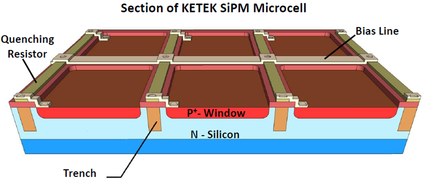
The most popular detector from this generation – SiPM – has been developed by the MEPhI/Pulsar collaboration led by Prof. B. Dolgoshein. The SiPM of this kind was very attractive due to the simplicity of its design and the ability to be reliably produced using semiconductor technology of moderate level. The negative feedback element in SiPM was realized as a thin-film polysilicon strip resistor connecting each individual APD pixel to a common electrode and located between pixels.
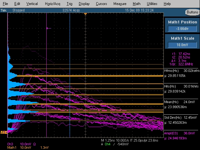
Photon number resolving response of SiPM (Hamamatsu MPPC) to short multi-photon light pulse (S. Vinogradov)
Since the mid-2000s, the SiPM design with polysilicon resistors became a conventional ground for an emerging wave of SiPM developments by Hamamatsu Photonics, SensL, FBK, STMicroelectronics, Excelitas Technologies, KETEK, and some others.
So, after all, the SiPM appears to be rather similar to a SPAD array with passive quenching, but with a much faster pixel recovery and much higher fill factor. In turn, the success of SiPM technology has inspired the re-invention of a SPAD array detector, using the achievements of modern CMOS technology and advancing its readout architecture in the so-called digital SiPM (dSiPM) developed by Philips in 2009, where the main drawback of SPAD arrays – low fill factor – was improved to about 50%.
The ANF concept and SiPM technology were also accepted by developers of non-silicon, first of all, the near-infrared (NIR) APDs starting since the mid-2000s in the USA. The designs have been adapted to III-V compound technology utilizing negative feedback based either on thin film resistor (Princeton Lightwave) or on charge accumulation at heterointerfaces of III-V layers (Jet Propulsion Laboratory, UCSD, UCLA).
Recently, an expansion of the SSPM into ultraviolet (UV) wavelengths and harsh environment operation has been possible through the development of a SiC-based UV SSPM (GE Global Research Center, 2014).
The overwhelming success and worldwide recognition of SiPM technology are due to its unprecedented performance at room temperature in a photon number resolution of multi-photon pulses, as well as, to its arrival time resolution. Highly beneficial features are the low operating voltages, insensitivity to magnetic field and to nuclear counter effect, scalability in creating large arrays, and its robustness and reliability for years, unaffected by occasional over-lighting. Now SiPM is approaching to be a real working horse for a variety of scientific and industrial applications, and mass-production pricing facilitates this progress.
However, conventional SiPM design has some drawbacks, for example the trade-off between density of pixels (dynamic range) and fill factor (detection efficiency), multiple trade-off dealt with pixel area – gain – pulse width – recovery time – crosstalk – after pulsing. Some of them are subjected to ongoing countermeasures and improvements, and some are inherent ones. There is room for alternative designs, thus a number of proprietary designs have been developing so far (Zecotek, Max Plank Institute, Novel Device Laboratory, ASTAR Institute of Microelectronics, and some others).